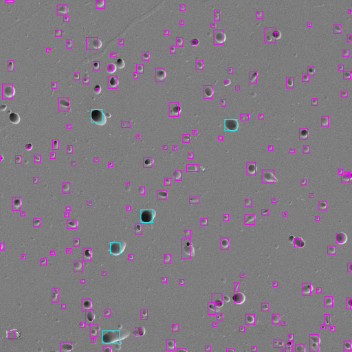
AI + SEM Track Detection
Automated CR-39 Track Analysis
Reading a CR-39 nuclear track detector by hand means counting etched tracks in a handful of microscope fields of view and extrapolating to the whole chip. It is slow, subjective, and blind to variation across the detector surface. BlankSlate Innovation replaces that workflow with SEM large-area mapping combined with an AI-driven track classifier that counts and characterizes tracks across the entire chip.
Automated optical readers solve the counting problem too, but they mean a capital purchase, a trained operator, and optical-resolution limits. With BSI there is no reader to buy: send exposed chips to us for full analysis, or work with us on experiment design, etching, and imaging so you capture the cleanest data. The methodology is validated in our peer-reviewed paper on AI analysis of CR-39 with SEM large-area mapping.
What you get back
From Exposed Chip to AI-Labeled Tracks
The ship-back analysis service runs your exposed CR-39 through the SEM large-area mapping pipeline and the AI-driven track classifier, returning quantitative, reproducible results across the whole detector. Order as little as a particle count or as much as the full set below. Every analysis includes source-versus-noise discrimination, which separates genuine tracks from polishing artifacts and surface contamination.
Particle Count & Flux
Tracks counted across the entire chip area, not just sampled fields of view, so there is no extrapolation error. Reported as counts or flux.
Particle Species
Alpha, proton recoil, and fission fragment tracks classified by the AI, not just counted as undifferentiated marks.
Energy Distribution
Particle energies derived from track diameter, length, and morphology in the high-resolution SEM maps.
LET Distribution
Linear energy transfer spectra for dosimetry and radiation-effects work.
Angle of Arrival
Incidence direction of individual particles, taken from track shape, so you can reconstruct source geometry.
Raw Track Data
Track images and per-track measurements, so you can run your own analysis alongside ours.
Turnaround: 10–30 days from receipt of your chips, depending on the complexity of the analysis and the number of samples. Pricing is quoted per project.
Head to head
Three Ways to Read CR-39
Manual microscopy is fine for a quick look. Automated optical readers such as TASLImage, RadoMeter, and Politrack are built for labs that process large, steady volumes in-house. BSI's ship-back SEM + AI service gives you automated full-chip analysis without buying or running a reader. Here is how they compare.
| Manual Optical Microscopy | Automated Optical Reader | BSI SEM Large-Area Mapping + AI | |
|---|---|---|---|
| What you need in-house | Microscope and an operator's time | A purchased reader system, a trained operator, and your own etching setup | Nothing — ship exposed chips to BSI |
| Area analyzed | Sampled fields of view, extrapolated to the chip | Large scanned areas at optical magnification | Full chip area, tiled into a single SEM map |
| Track counting | Manual, operator-dependent | Automated | Automated and reproducible |
| Resolution of fine track detail | Limited by optics | Limited by optics | Scanning electron microscope resolution |
| Particle-type identification | Operator judgement | From measured track size and shape parameters; varies by system | AI classification: alpha, proton recoil, fission fragment |
| Energy information | Rarely quantified | Available on some systems from track parameters | Energy distribution from track diameter, length, and morphology |
| Other outputs | — | Per-track parameters; varies by system | LET distribution, angle of arrival, raw track images and per-track data |
| Turnaround | Your own schedule | Your own schedule, once the system is set up | 10–30 days from receipt, depending on complexity and sample count |
| Artifact rejection | Manual, inconsistent | Rule-based filtering; varies by system | AI source-vs-noise discrimination |
| Best fit | Quick checks, teaching | High-volume routine processing, such as dosimetry services and radon labs | Research projects, variable or occasional volumes, publishable datasets |
| Validation | Lab-specific | Manufacturer and user publications | Peer-reviewed (doi.org/10.1016/j.net.2025.103738) |
TASLImage, RadoMeter, and Politrack are products of Track Analysis Systems Ltd, Radosys, and Mi.am respectively, named only to identify the category. Capabilities vary by model and configuration; check with each manufacturer for specifics. BSI is not affiliated with any of them.
The workflow
How the Ship-Back Service Works
BSI supports the full CR-39 workflow — run the experiment yourself with our guidance, or ship exposed chips back to us for imaging and AI analysis.
01
Experiment Design
We help set up exposures, geometries, and shielding for your particle type, energy range, and source strength.
02
Etching
Optimize NaOH concentration, temperature, and etch time for alpha tracks, fission fragments, proton recoil, or boron-coated thermal-neutron capture.
03
SEM Large-Area Mapping
High-magnification SEM images are tiled into a single map of the whole etched surface for reliable large-area coverage.
04
AI Classification
The AI classifier delivers counts, particle-type identification, energy estimates, and artifact rejection.
Prefer to run your own imaging? We also advise on optical and electron microscopy procedures, magnification, contrast, and tiling strategies to produce reliable large-area maps in your own lab. See the CR-39 best-practice guide for handling, etching, and imaging detail.
Questions researchers ask
CR-39 AI Analysis FAQ
Can AI analyze CR-39 nuclear track detectors?
Yes. BSI pairs SEM large-area mapping with an AI-driven track classifier to analyze exposed CR-39 chips. The AI locates and counts etched tracks across the full chip area, identifies particle type, and estimates energy from track morphology. The methodology is documented in BSI's peer-reviewed paper on AI analysis of CR-39 with SEM large-area mapping.
How do I automatically count tracks on CR-39?
Rather than manually counting a few sampled fields of view under an optical microscope, you can send exposed CR-39 chips to BSI. The SEM large-area mapping pipeline images the whole chip and the AI classifier returns a particle count across the full chip area, not just sampled regions. This removes the sampling extrapolation and subjective counting that limit manual optical methods.
What is SEM large-area mapping of CR-39?
SEM large-area mapping is a scanning electron microscopy workflow that tiles many high-magnification images together into a single map covering the entire etched CR-39 surface. It resolves fine track detail that optical microscopy can miss, and provides the high-resolution imagery the AI classifier uses to count and characterize tracks. You can explore an interactive example of a CR-39 chip exposed to Am-241 alpha particles here.
Can the AI tell alpha tracks from proton recoil or fission fragments?
Yes. The AI track classifier performs particle-type identification, distinguishing alpha tracks, proton recoil, and fission fragments. It also estimates energy from track diameter, length, and morphology, and applies source-versus-noise discrimination to separate genuine particle tracks from polishing artifacts and surface contamination. See an example of AI-detected U-238 fission-fragment tracks here.
How long does analysis take, and what do I get back?
Turnaround is 10–30 days from receipt of your chips, depending on the complexity of the analysis and the number of samples. Results can be as simple as a particle count or flux, or can include particle species, energy distribution, LET distribution, angle of arrival, and raw data from the track images. Pricing is quoted per project.
How does this compare with an automated optical reader such as TASLImage, RadoMeter or Politrack?
Automated optical readers are purchased systems that scan etched detectors quickly at optical resolution and measure track size and shape; they suit labs that process large, steady volumes of detectors in-house. Our ship-back service needs no equipment purchase or trained operator: you send exposed chips, and we etch them, map the whole chip with a scanning electron microscope, and use an AI classifier to count tracks, identify particle type (alpha, proton recoil, fission fragment), estimate energy, and reject artifacts. It suits research projects, variable or occasional volumes, and datasets headed for publication.
Do I have to buy the detectors from BSI to use the analysis service?
BSI manufactures CR-39 detectors (standard chips at $2/cm2 and boron-coated chips at $5/cm2) and offers a ship-back SEM and AI analysis service. You can order chips, request analysis of exposed chips, or both. Describe your exposure conditions and what you are trying to detect on the CR-39 service request form, and BSI advises on experiment design, etching, and imaging.
Get started
Order Chips or Start an Analysis Project
Tell us how many chips you need, whether you want boron coating, and what you are trying to detect. For ship-back analysis, describe the exposure conditions and what you are looking for in the data.
Related: passive neutron detection · CR-39 for teaching labs · published research · switching from TASTRAK · international customers