Electronic System Design
Below are some examples of our electronic system design.
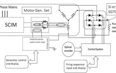
System for Extracting Electrical Energy from Inertial Energy of Rotational Devices
System for Extracting Electrical Energy from Inertial Energy of Rotational Devices
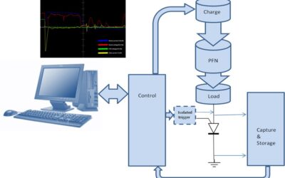
Narrow-Pulse Test Bed for Evaluation of Experimental Wide Bandgap Semiconductor Devices
Narrow-Pulse Test Bed for Evaluation of Experimental Wide Bandgap Semiconductor Devices
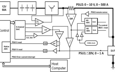
High Current Device Characterizer
High Current Device Characterizer
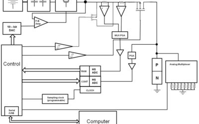
Open-Circuit Voltage Decay System
Open-Circuit Voltage Decay System
High-Current Digitally Controlled Pulser for High Magnetic Field Applications
High-Current Digitally Controlled Pulser for High Magnetic Field Applications
Low-Noise Universal Power Supply
Low-Noise Universal Power Supply
Sensor Integration Block
Sensor Integration Block
Fourier-Transform Ion Cyclotron Resonance Mass Spectrometer
Fourier-Transform Ion Cyclotron Resonance Mass Spectrometer
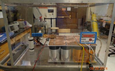
Low Inductance Double Pulse Test Bed
Low Inductance Double Pulse Test Bed
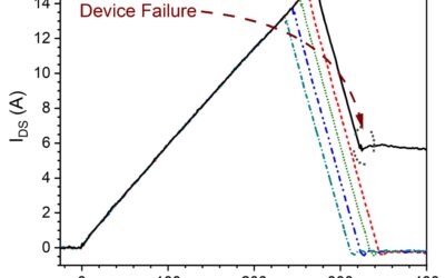
Wide Bandgap Avalanche Energy Test Bed
Wide Bandgap Avalanche Energy Test Bed
System for Extracting Electrical Energy from Inertial Energy of Rotational Devices
System for Extracting Electrical Energy from Inertial Energy of Rotational Devices
This system was designed to extract electrical energy from the mechanical inertia of rotational machines in a pulsed-power (fast) manner.
Block diagram:

Physical system:

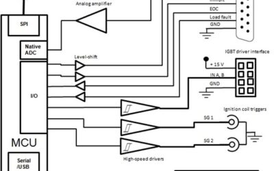
Narrow-Pulse Test Bed for Evaluation of Experimental Wide Bandgap Semiconductor Devices
Narrow-Pulse Test Bed for Evaluation of Experimental Wide Bandgap Semiconductor Devices
This system performs automated high-energy repetitive stress-cycling of experimental semiconductor devices, recording all pertinent waveforms with built-in, high frequency data acquisition and alternates device characterization at chosen intervals via a bult-in, high voltage, high current curve tracer, switching between the two sets of circuitries with a custom-designed 3-pole, 3-throw electromechanical switch.
Block diagrams:


Physical system:

High Current Device Characterizer
High Current Device Characterizer
This high current characterization system is comprised of two independently controlled power supply units; PSU1 and PSU2. PSU1, a +- 20 V at 1 A supply is intended principally for powering the control lead of a three terminal device, or it can be used for relatively low current tracing (<= 1 A). This supply can be operated in either a pulsed or a continuous manner. PSU2 is a 10 V @ 500 A max supply that operates only in a pulsed mode. The output of PSU2 is produced by a high power linear amplifier with feedback that utilizes paralleled Insulated Gate Bipolar Junction Transistors (IGBTs) as series – pass elements. The unit derives IV characteristics for very high-current devices.
Block diagram:

Physical system:

Open-Circuit Voltage Decay System
Open-Circuit Voltage Decay System
This system performs open circuit voltage decay analysis on packaged PN junction devices for use with injection-dependent lifetime spectroscopy techniques. The system injects currents that can range from ~ 1 mA to 100 A in a pulsed manner through an electronically controlled, fast, nearly ideal switch to disconnect the device being analyzed. Data is acquired and uploaded to a custom program that automates much of the analysis required for carrier lifetime spectroscopy.
Block diagram:

Physical system:

High-Current Digitally Controlled Pulser for High Magnetic Field Applications
High-Current Digitally Controlled Pulser for High Magnetic Field Applications
The high-current pulser system drives a specially designed coil to achieve fast, controllable magnitude and pulse-width magnetic fields in the 0 to 5 Tesla range.
Block diagram:

Physical system:

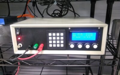
Low-Noise Universal Power Supply
Low-Noise Universal Power Supply
This system is a custom constant-voltage, constant-current, very low-noise, digitally controllable power supply with a built function generator and the ability for external modulation of current or voltage. Custom software was also written for PC control of the unit.

Physical system:


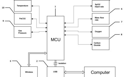
Sensor Integration Block
Sensor Integration Block
The Sensor Integration Block (SIB) may be inserted in-line between a respiratory mask and any commercially available CPAP, respirator or breathing device. A portable version has also been produced for field deployment. This SIB records, logs, and analyzes a comprehensive dataset, and displays this data on custom Windows-based software.
Block diagrams:


Physical system:

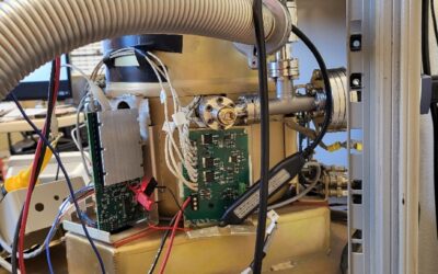
Fourier-Transform Ion Cyclotron Resonance Mass Spectrometer
Fourier-Transform Ion Cyclotron Resonance Mass Spectrometer
Complete custom electronic systems designed around a “smart module” philosophy where each hardware function is autonomous, and directed by a main module. A custom software suite is used to control settings and read data.
Block Diagram:
Module-level Block Diagrams:
Physical System:
Low Inductance Double Pulse Test Bed
Low Inductance Double Pulse Test Bed
A low inductance double pulse tester was developed to analyze the switching characteristics of SiC MOSFET modules. The parallel configuration of the modules enables high current operation, however, a compatible power supply unit is often difficult to acquire. With a desired operating current of 300 A peak, a cost effective solution was to implement a capacitor bank as an energy source. A low inductance design was selected to minimize the effect of parastic inductance on measurement integrity. The system was designed to provide pulse widths up to 400 µs with a maximum current droop of only 2 %; maximum design energy was ≈ 7 kJ.


Wide Bandgap Avalanche Energy Test Bed
Wide Bandgap Avalanche Energy Test Bed
Custom electronic testbed utilized for the evaluation of avalanche energy tolerance of wide bandgap semiconductors. A modular design approach was utilized to allow for a wide variety of control conditions to be implemented in addition to varying package topologies. An important design aspect implemented was precise energy control allowing the failure mode to be analyzed post destructive failure. Both commercial and research grade Silicon Carbide (SiC) MOSFETs were evaluated.

