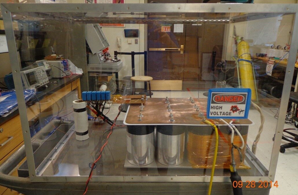
Low Inductance Double Pulse Test Bed
A low inductance double pulse tester was developed to analyze the switching characteristics of SiC MOSFET modules. The parallel configuration of the modules enables high current operation, however, a compatible power supply unit is often difficult to acquire. With a desired operating current of 300 A peak, a cost effective solution was to implement a capacitor bank as an energy source. A low inductance design was selected to minimize the effect of parastic inductance on measurement integrity. The system was designed to provide pulse widths up to 400 µs with a maximum current droop of only 2 %; maximum design energy was ≈ 7 kJ.

